Bypassing the Renesas RH850/P1M-E read protection using fault injection
Introduction
In this blog post, I'll describe a fault injection attack to read the flash contents of a Renesas R7F701381 (RH850/P1M-E series) that has programmer access disabled. This microcontroller is meant for safety critical applications (ASIL-D) and has a second core that can run in lockstep and checks the first core. The instruction cache and RAM have ECC functionality.
The reason for this project is that I'm trying to dump the the firmware from the Electronic Power Steering (EPS) module from a 2021 Toyota RAV4 Prime. This is one of the new Toyotas using Autosar's new Specification of SecureOnboard Communication (SecOC) standard to authenticate CAN messages. This means that the EPS no longer accepts spoofed CAN messages from a third party device. Hopefully I'll be writing more about this in the future.
Unfortunately this car was too rare for parts to show up at the scrapyards, so the part had to be bought new ($$$). The Hyundai and Honda EPS modules I looked at in the past left their debug access wide open, but that wasn't the case for this EPS. This meant that just reading the firmware was going to be the first challenge for solving this SecOC problem.
The inspiration for the fault injection attack came from Franck Jullien's great research on the Renesas RX65. However, this attack is different in a few aspects. The RH850 uses the V850 architecture instead of RX, which means the boot ROM is probably different. I'm using the two-wire (UART) debug interface, instead of the single-wire FINE interface. Franck also has to bypass an ID code (password) check, while on this device the programming interface itself was "disabled"1.
Other interesting research was done by Collin O'Flynn on the NXP MPC55xx and MPC56xx in his 2020 paper: "BAM BAM!! On Reliability of EMFI for in-situ Automotive ECU Attacks". In this paper he is able to bypass the password check in the Boot Assist Module using ElectroMagnetic Fault Injection. This research is relevant since the MPC55xx/MPC56xx is also an automotive chip and has similar ASIL-D safety features as the RH850/P1M-E.
First I'll describe the debug protocol used by this chip. Then I'll introduce Fault Injection, and describe the hardware and software used in this attack. All code used in this post can be found on GitHub.
Two-wire debug protocol
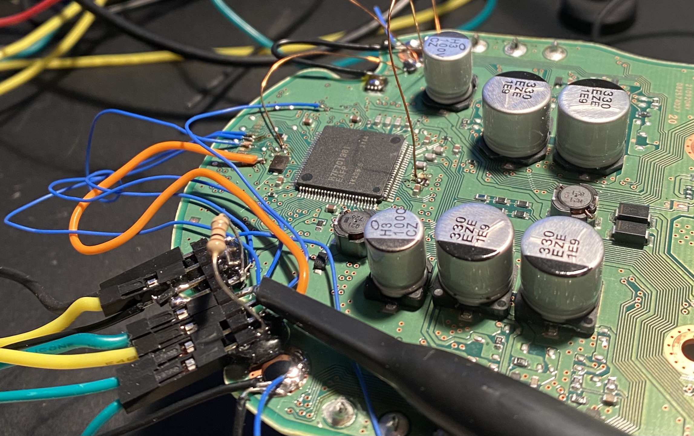
The first step in reading the firmware was hooking it up to the computer. Fortunately, this Renesas chip supports a two wire protocol which can be hooked up to the computer using a standard 5V USB-TTL cable. To enable the debug mode, you just have to pull the FLMD0 pin high using a pull-up resistor. JP0_0 and JP0_1 have to be connected to RX and TX on the USB-TTL adapter.
When working with microcontrollers used in safety critical applications, you always have to be aware of external watchdogs. This was also the case for this EPS. If the external watchdog isn't happy it will forcibly reset the microcontroller by briefly pulling down the reset line. Quickly after entering the bootloader the chip would be reset. This was fixed by forcing the reset line high by attaching a 100 ohm resistor to +5V, which was enough to overpower the external watchdog. To still be able to control the reset line I added an N-FET between reset and GND, which could be controlled using software with the DTR line on the USB-TTL adapter.
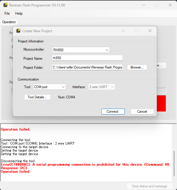
A bit of soldering later everything was hooked up, and I could communicate using the Renesas Flash Programmer. Unfortunately, it wasn't this easy, and I got a message saying "A serial connection is prohibited for this device.". Before I can try to bypass this, I first need to understand the protocol between the Flash Programmer and the device. This gives insight into possible weaknesses, and allows me to build my own implementation of the flasher.
Even though there is no documentation for my exact chip, you can learn a lot from documentation of other chips. Renesas uses a similar implementation of the same debug protocol across many chips. In this case the "RX65N Group, RX651 Group User's Manaual: Hardware" (section 59.13, Boot Mode Communications Protocol) and the Application Note "System Specifications for Standard Boot Firmware for the Renesas RA family" turned out to be very useful. There is also a Python implementation by Greg Hogan for the V850 and SH72.
After hooking up the logic analyzer and trying to connect, I can observe the communication between the PC and the device. Commands come in two flavors: one where the reply is a simple OK, and one where you can ask for more data. Commands start with either 0x01 or 0x81, followed by a two byte length. Each packet ends with a 1 byte checksum2 and a constant 0x03.
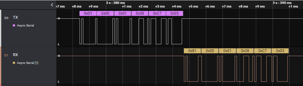
In the following example with command 0x32 (frequency setting command) you can see that the device returns a simple ACK, but when echoing back that same ACK it sends the actual data. This will be relevant later when trying to use the read command to read flash memory.
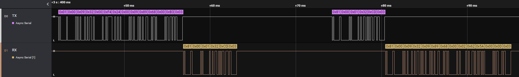
The Renesas Flash Programmer GUI first goes through a few steps where it sets up device clock frequencies and baud rate. Then, it sends a "synchronize" command, which gives returns error 0xDC (serial programming disable error). If you skip any of these steps, or try to issue a read command without calling synchronize, you get error 0xC3 (flow error). This is further confirmed by the flow chart from the RX65 datasheet, which shows all the steps needed to enter the command waiting phase where you should be able to issue read commands. Looking at flow chart I got the idea that the synchronize command is the only place where the device checks if the connection of a programmer is allowed. If you manage to jump to the command waiting phase, you should be able to do whatever you want.
Fault Injection
Fault injection is a method where you run a CPU outside of the normal ranges of operation. This can be done by (very briefly) changing the operating voltage (voltage glitching) or clock frequency (clock glitching). It's also possible to influence behavior by sending electromagnetic or laser pulses into the chip.
Both voltage and clock glitching can be done with relatively cheap hardware such as an FPGA or even a small microcontroller and few external parts.
The main goal of fault injection is to influence the behavior of the microcontroller. That can either happen due to outright skipping instructions, or causing memory reads/writes to fail.
In this case, I'm going to perform a voltage glitch on the power supply circuit of the microcontroller. By shorting the power supply for 100 ns or less, you can modify the behavior of a very specific part of the running program.
Specifically, I'm targeting the part where it checks if programming is enabled after receiving the synchronize command. The time between the last byte of the command and the first byte of the response is about 100 μs. Given the short duration of the glitch it can take quite a while to find the correct timing for the fault injection.
Voltage Glitching - Hardware
In section 9.3.1 of the RH850 datasheet, a block diagram for the power supply circuit is shown (see image below). You can see the voltage for the CPU core (digital circuits) is generated by an internal 1.25 V regulator (labeled eVR in the diagram). To stabilize the voltage, it's brought out on an external pin to attach a capacitor (VCL). This pin is a very convenient point to perform a fault injection. It should have minimal effect on the rest of the chip's peripherals and it's not checked by the core voltage monitor.
Since the RH850 is used in safety critical applications, it has a second core that functions as a checker. There are two VCL pins, probably one for each core. They probably need to be glitched at the same time to achieve the desired results. Otherwise, the result is probably that the cores get out of sync and the device resets.
The decoupling capacitors are removed from both VCL pins, which would otherwise smooth out the glitches. Then both VCL pins are connected to an N-FET (DMN2050L is what I had lying around, but any fast N-FET works) driven by a Raspberry Pi Pico. A picture of the PCB is shown below. The two N-FETs are glued to the board and attached using a short wire. The connector on the bottom left is used for connecting to the debug interface.
Voltage Glitching - Software
The glitch is generated by an Raspberry RP2040 with a few lines of code. The important part of the firmware is as simple as:
if (uart_getc(uart0) != '\x01') continue;
if (uart_getc(uart0) != '\x00') continue;
if (uart_getc(uart0) != '\x01') continue;
if (uart_getc(uart0) != '\x00') continue;
if (uart_getc(uart0) != '\xff') continue;

busy_wait_at_least_cycles(real_delay);
gpio_put(GLITCH_PIN, 1);
busy_wait_at_least_cycles(width);
gpio_put(GLITCH_PIN, 0);
The RP2040 waits for the synchronize command (minus the last \x03), waits a bit and then generates a short pulse. The rest of the firmware handles configuring the delay and width of the pulse over USB.
On the PC side there is a python script that implements the debug protocol and controls the RP2040. It keeps trying to get past the synchronize command, and loops over a wide variety of glitch parameters. After about a day of trying I got the first success. After I had a rough idea of the glitch parameters, each subsequent attempt only took 5 to 30 minutes.
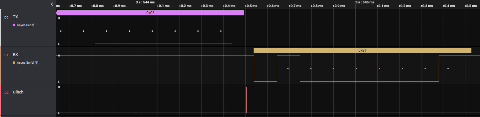
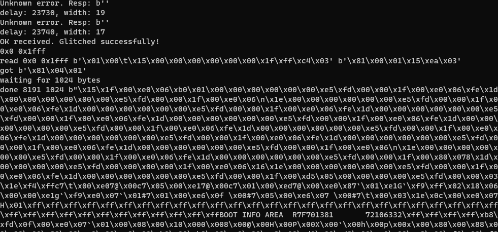
After getting past the synchronize command, it was indeed possible to issue read memory commands! After spending some time to figure out the right start and end addresses (the command only works on whole 8kb/32kb blocks) I was able to dump the whole firmware.
update 2022-11-09:
I also tried glitching only a single VCL pin. Glitching just the single VCL on pin 11 also seems to work. However, when glitching just the VCL on pin 66 I can get past the synchronize command, but then memory reads still fail with a flow error. This effect is probably due to the setup with a main core and a checker core, although I'm not exactly sure why a glitch on the checker core leads to any result at all.
Conclusion
With this attack it's possible to bypass the programmer disabled setting on the RH850/P1M-E. It doesn't require complex hardware, and can be done without desoldering the microcontroller.
I noticed that the length of the glitch required to get any results would often lock up the whole microcontroller requiring a full reset. In this case there was no further ID-Code or password set to protect the interface. Even though that might sound redundant, it would have increased the complexity of the attack quite a bit due to requiring two subsequent glitches.
In this attack, I glitched past the synchronize command to issue a read command on a device where programming interface has been disabled. It might also be possible to glitch the read command itself, in order to read protected areas. However, to dump the whole firmware that would require a successful glitch for every 32kb of flash. This might be a good way to extract the boot ROM though.